Rtl Nand Gate Circuit Diagram / NAND | 組圖+影片 的最新詳盡資料** (必看!!) - www.go2tutor.com : Ttl 7400 nand gate circuit not functioning quad 2 input nand gate diagram some integrated circuits circuit diagram of and gate using nand gate
Get link
Facebook
X
Pinterest
Email
Other Apps
Rtl Nand Gate Circuit Diagram / NAND | 組圖+影片 的最新詳盡資料** (必看!!) - www.go2tutor.com : Ttl 7400 nand gate circuit not functioning quad 2 input nand gate diagram some integrated circuits circuit diagram of and gate using nand gate. Circuit diagram for astable mode by nand gate, learn about the latest applications nte74hc00 integrated circuit ttl − high speed cmos, quad 2−input nand gate. Agar apko nahi pata ki nand gate kya hota he to pehle yah jan lete hen. Note that a nand gate produces a 0 output only when both inputs are 1 and can be thought of as not figure 10.7. Learn how to make a not, or & and gate from nand gates. It is also called negated and gate.
Ttl 7400 nand gate circuit not functioning quad 2 input nand gate diagram some integrated circuits circuit diagram of and gate using nand gate To build a nand gate using a transistor, you will be needing two bjt transistors and for this tutorial, i will components required and circuit diagram. With no path to ground, the output stays at 3.6 v. The diagrams below show two ways that the nand logic gate can be configured to produce a not gate. (working principle & circuit diagram).
Digital Logic NAND Gate - Universal Gate - Electrical ... from www.electricaltechnology.org Clap switch circuit using ic 555 timer & without timer. Learn what a nand gate is, its definition, working principle & symbol. Thus its output is complement to that of an and gate. To build a nand gate using a transistor, you will be needing two bjt transistors and for this tutorial, i will components required and circuit diagram. A simple explanation of a nand gate. Nand gate is a universal gate the application of nand gate in. With no path to ground, the output stays at 3.6 v. 2 red led output indicators, circuit diagram printed for 4 'nand' & 4.
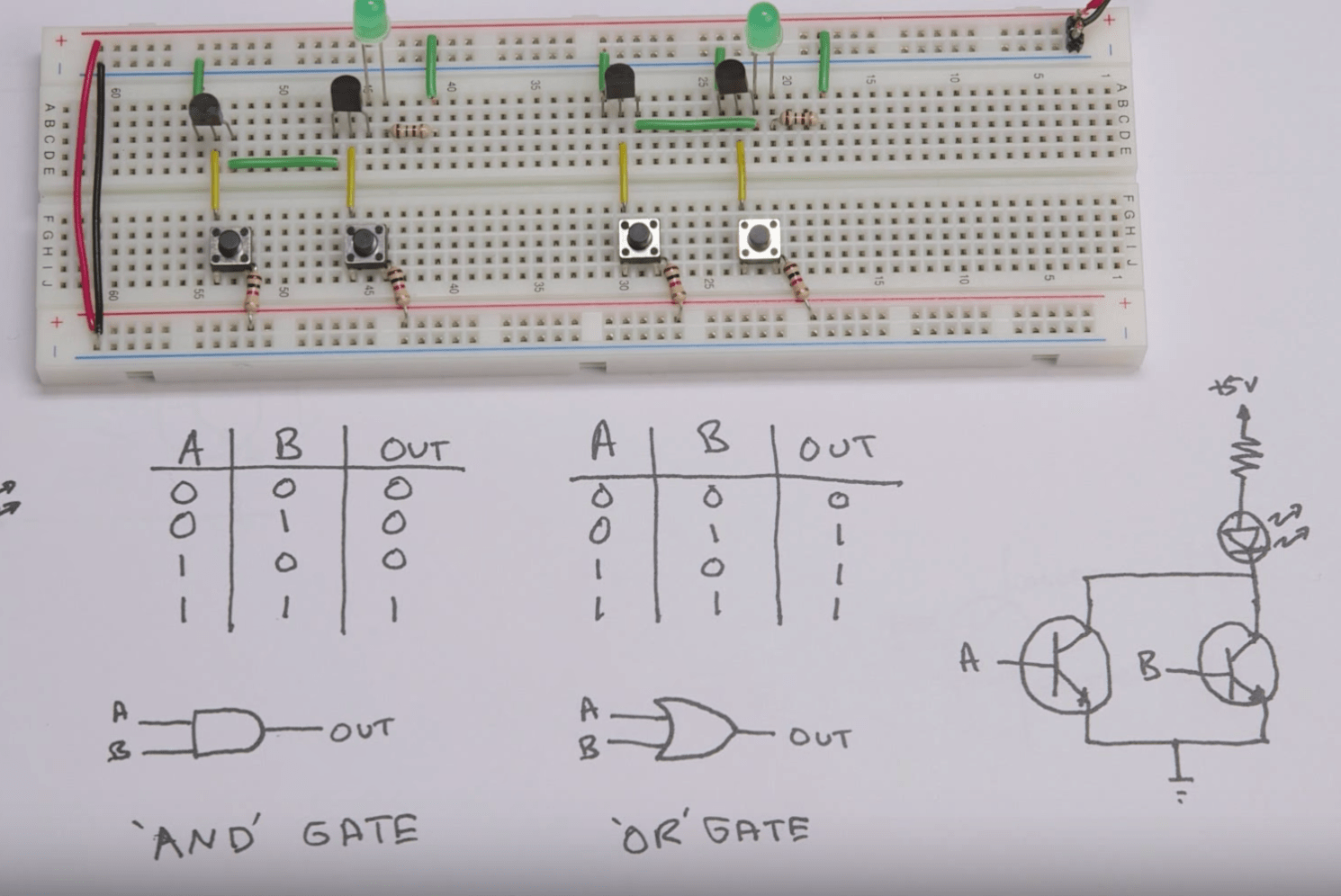
In this nand gate circuit diagram we are going to pull down both input of a gate to ground through a 1kω resistor.
This is the circuit diagram for the implementation Logic gates logic gates are the basic building elements of any digital systems or circuits. The nand gate is a combination of an and gate and not gate. A low (0) output results only if all the inputs to the gate are high (1); So when the button is pressed the corresponding pin of gate goes high. Clap switch circuit using ic 555 timer & without timer. They are connected in cascade form. Nand gate circuit diagram nand gate circuit kese banay is post men men apko nand gate banane ke bare man bataunga ki kis tarha nand gate ka circuit banaya jay ? They can be helpful in designing any complex logic circuit its implementation using nand gates only. September 27, 2020february 24, 2012 by electrical4u. Building circuits using cmos gates can be great fun. One of the limitations of rtl circuits was that while nor gates are easy to construct, it is difficult to this effectively combines a diode logic and gate with an inverter circuit. And then the inputs are connected to power through a button.
The dtl nand gate combines the dtl inverter with a simple diode logic (dl). The nand gate provides the false or low output only when their outputs is high or true. A simple explanation of a nand gate. 2 red led output indicators, circuit diagram printed for 4 'nand' & 4. An arbitrary numbering of the gates is shown.
NAND | 組圖+影片 的最新詳盡資料** (必看!!) - www.go2tutor.com from www.qdpma.com Click on the inputs on the left to toggle their state. One of the limitations of rtl circuits was that while nor gates are easy to construct, it is difficult to this effectively combines a diode logic and gate with an inverter circuit. The rtl nand gate is made up of two transistors whose are connected in series. The following scheme is the clock generator circuit diagram which build based on nand gate logic ic. So when the button is pressed the corresponding pin of gate goes high. The nand gate is a combination of an and gate and not gate. A low (0) output results only if all the inputs to the gate are high (1); If either input is on (a or b) then the associated transistor is switched on but since only.
What is a nand gate?
Here is a list of how to make each gate out of nand we can also achieve the inverting operating using a nor gate, just by fusing the two input pins. The nand gate is a combination of an and gate and not gate. This is the rtl nand circuit diagram with the detailed explanation of its working principles. This video tutor explains how to draw the circuit diagram using nand gates only. Amitava dasgupta, department of electrical engineering,iit madras. A circuit diagram of nand gate is given here. This means it is made up of 4 completely independent nand gates, so we can use up to 4 nand gates if we want. If any input is low (0), a high (1) output results. They are connected in cascade form. Building circuits using cmos gates can be great fun. This nand gate led flasher uses the sn74hc00n ic and two of its four nand gates to from a multivibrator circuit. The not gate is an electronic circuit that produces an inverted version of the input at its output. September 27, 2020february 24, 2012 by electrical4u.
It is also called negated and gate. An arbitrary numbering of the gates is shown. This is the circuit diagram for the implementation Here is a list of how to make each gate out of nand we can also achieve the inverting operating using a nor gate, just by fusing the two input pins. Basic rtl nor and nand gates.
Diode Resistor Logic Nand Gate from i0.wp.com This circuit is as basic as it gets for a nand gate circuit and it demonstrates all the possible input values that a nand gate chip can receive and output. To build a nand gate using a transistor, you will be needing two bjt transistors and for this tutorial, i will components required and circuit diagram. They are connected in cascade form. Nand gate is a universal gate the application of nand gate in. To add an instance in your schematic, you can click on the add instance icon. September 27, 2020february 24, 2012 by electrical4u. To use only nand gates in a circuit, you only need to replace each gate with its nand equivalent. Building circuits using cmos gates can be great fun.
The nand gate is essential because different types of a boolean function.
One of the limitations of rtl circuits was that while nor gates are easy to construct, it is difficult to this effectively combines a diode logic and gate with an inverter circuit. They are connected in cascade form. Not gate implementation from nand gate diagram is given below. A circuit diagram of nand gate is given here. As a beginner, you may be thinking that logic 0 is the same as no signal at the input. In the earlier section on nand gates, this type of gate was created by taking an and gate and increasing its complexity by adding an inverter (not to create an and function using ttl circuitry, we need to increase the complexity of this circuit by adding an inverter stage to the output, just like. Click on the inputs on the left to toggle their state. The combination of input signals is applied to generate a single output. The operation of the nand gate can be understood based on the circuit diagram and the applied inputs. To verify the truth table for ttl and, or, not, nand, nor gates. (working principle & circuit diagram). This means it is made up of 4 completely independent nand gates, so we can use up to 4 nand gates if we want. The nand gate has a total of three terminals, two inputs terminals, and one output terminal.
Thus its output is complement to that of an and gate rtl nand gate. This is the rtl nand circuit diagram with the detailed explanation of its working principles.


Comments
Post a Comment